5G Electronics Laser Precision
High-speed, micron-level laser cutting, drilling, and welding solutions designed to overcome advanced material and high-density integration challenges in 5G telecommunication hardware manufacturing.

The 5G Electronics Industry Demands Ultimate Precision
5G telecommunications hardware operates under demanding high-frequency, high-speed standards. To minimize signal loss and support massive MIMO, electronics manufacturing utilizes highly sensitive low-κ dielectrics, LCP, MPI films, and dense HDI boards.
Traditional mechanical tools cause severe thermal damage, delamination, and physical stress on these fragile materials. Precision laser manufacturing delivers non-contact, micro-scale processing, preserving structural integrity and RF performance while achieving the micro-vias, ultra-fine contours, and defect-free singulation required for next-generation 5G hardware.
Key 5G Electronics Manufacturing Challenges
Addressing the top physical, thermal, and micro-precision bottlenecks in high-frequency 5G communication electronics manufacturing.
-

LCP/MPI Antenna Thermal Damage
High-frequency antenna materials deform easily during mechanical punching. Laser processing cuts contours cleanly with negligible heat-affected zones.
-
Micro-Via Drilling in HDI
Dense 5G PCBs require micro-vias under 50µm, surpassing the precision and speed capability of traditional mechanical drills.
-
Low-κ Dielectric Brittle Cracking
Brittle low-κ substrates easily crack or delaminate under mechanical stress. Non-contact lasers eliminate physical impact and preserve materials.
-
Wafer Dicing Residual Stress
Traditional blade sawing chips thin 5G wafers. Laser dicing ensures kerf separation without debris, micro-cracks, or stress.
-
High-Pitch Optical Module Soldering
Solder joints down to 50µm pitch on high-speed transceivers suffer bridging and poor consistency during manual reflow.
-
Ceramic Substrate Micro-Cracking
LTCC/HTCC materials suffer low yield and micro-cracks under mechanical drilling. Laser drilling achieves clean, high-roundness micro-holes safely.


Laser Systems Engineered for 5G
High-precision laser systems optimized to deliver micro-scale cutting, drilling, and welding for high-volume 5G electronics production.

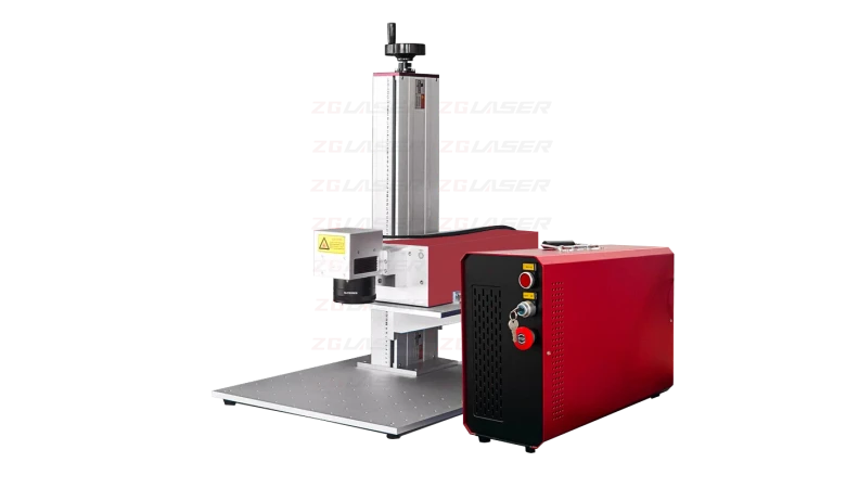
Picosecond UV Laser Cutting System
Advanced ultrashort-pulse UV laser solution, engineered specifically for cutting and routing delicate LCP, MPI, and FPC antenna materials with micron-level accuracy and minimal thermal impact.
- Heat-affected zone < 5µm
- 355nm UV wavelength prevents burning
- Integrated high-speed pulse-shaping technology

Precision Optical Module Laser Welder
A fully automated laser welding and micro-soldering system designed for SFP/QSFP optical transceivers, RF filters, and high-frequency communication modules with precise thermal feedback.
- Spots under 50µm diameter
- Automated vision-guided alignment
- Low-distortion dissimilar metal welding

High-Traceability Precision Laser Marking System
Ultra-precise laser marking solutions for permanent micro-text, QR codes, and barcodes on wafers, PCBs, ceramics, and plastics, fully integrated with MES tracking systems.
- Micro-text down to 0.1mm
- Dual-vision automatic positioning alignment
- Supports UV, green, fiber wavelengths
5G Laser Applications in Action
Real-world high-precision manufacturing processes where our advanced lasers drive down cycle times and maximize yield rates.
-
ANTENNA PROCESSING
LCP Film Cutting
Picosecond UV laser cutting of flexible LCP/MPI antenna films, preserving electrical properties and eliminating burrs or delamination.
-
HDI PCB
Micro-Via Drilling
Laser drilling of sub-50µm blind and through vias on multilayer HDI boards, doubling throughput compared to conventional drills.
-
CHIP PACKAGING
Wafer Stealth Dicing
Internal laser modification and tape expansion of thin 5G processor wafers, achieving zero-chipping and narrow 20µm kerf widths.
-
OPTICAL MODULES
Micro-Pitch Soldering
Sub-50µm spot laser soldering of transceiver pins and housings, ensuring high-speed automation with no thermal distortion.


Partner in 5G Laser Manufacturing
Drawing on 40+ years of industrial laser expertise, ZG Laser provides high-precision smart systems that help 5G electronics manufacturers overcome complex material limits and meet rigid global quality standards.
-
CE & ISO Certified
Equipment and processes validated for international telecommunication hardware.
-
400+ Patents
Proprietary technology ensuring cutting-edge laser processing performance.


AEROSPACE INSTALLATIONS
Explore Our Aerospace Product Range
-
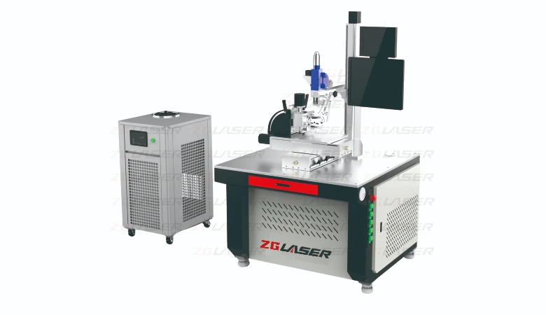
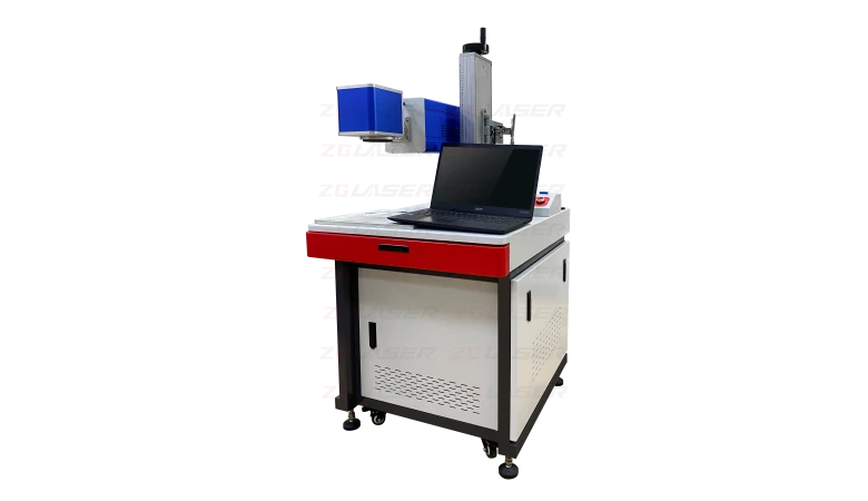
01Workbench Industrial Fiber Laser Welding MachineRed light positioning ensures high-precision welding performance. Modular design supports multiple welding modes and easy expansion. Compatible with industry fixtures, easy to connect with automatic lines
-
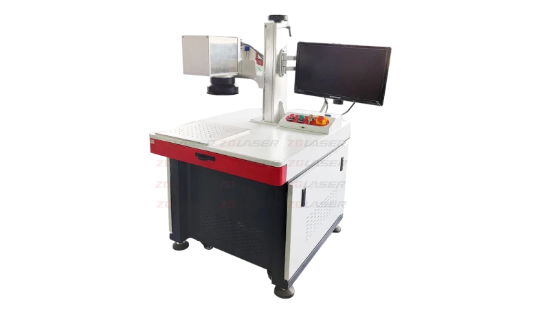
02High Speed Galvo Scanner Laser Welding MachineHigh-speed Galvo Scanner system achieves rapid precise positioning. Superior beam quality ensures flawless and firm welding joints. Optimized for precision batch welding of industrial metal components.
-
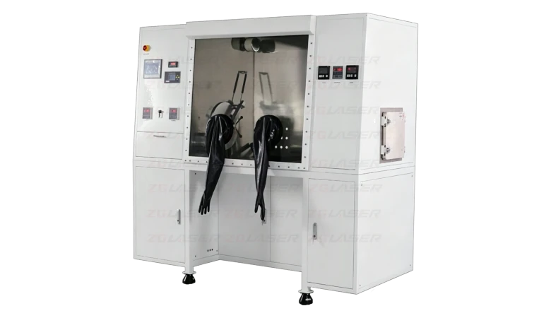
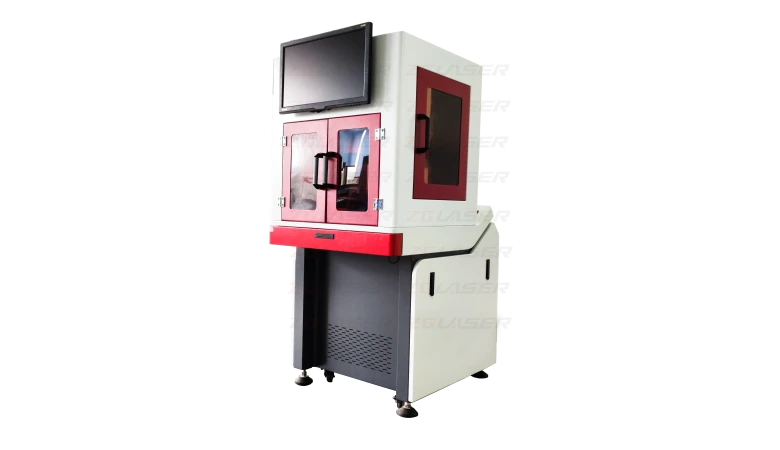
03Sealed Glove Box Laser Welding MachineSealed glove box structure achieves dust-free & clean welding. High-precision welding ensures smooth and firm welding seams. Safe & stable performance for high-standard precision components.
-
04UV Laser Marking MachineUltraviolet laser for ultra-fine, low-heat marking. Superior beam achieves delicate patterns without surface damage. Wide use for fragile materials and high-precision engraving.
-
05CO2 Laser Marking MachineHigh-precision marking and engraving for a wide range of non-metallic materials. Equipped with a stable CO2 laser source for consistent beam output and reliable long-term performance.
-
06Enclosed Fiber Laser Marking MachineFully enclosed housing ensures safe and dustproof operation. High-precision laser for clear and permanent marking. Ideal for clean workshop and high-standard production.